Failure analysis - Defective diode bridge - Acoustic microscopy
Examination realized by acoustic microscopy to check the interfaces integrity of a defective diode bridge module.
Regarding the interfaces, this assembly can be compared to an IGBT module.
The goal is to control the interfaces sole/solder, solder/alumina, solder between alumina and chip, chip/resin, and highlight indications like voids in solders and delaminations at interfaces.
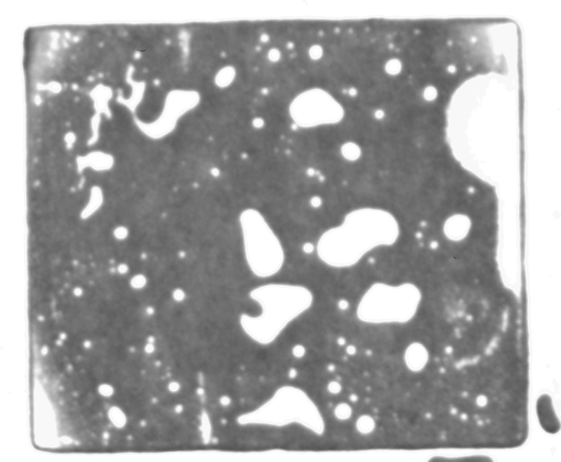
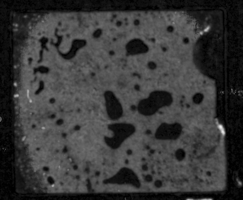
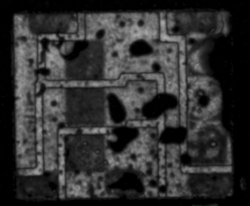
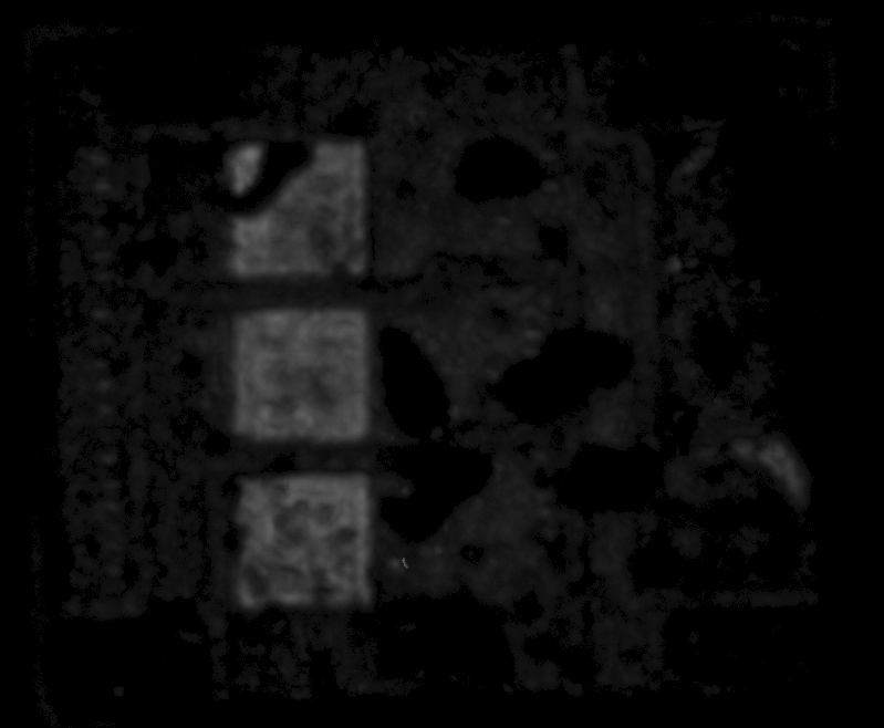
The images are done in emission mode at each interface level.
We can observe :
1-on the solder/alumina interface image, numerous white ovoïd indications significant of important voids in solder, the most important located in the edge of soldered area.
2-on the solder/alumina interface image, some very small white indications like voids at left and right edges. We can see attenuation (dark areas) indications detected at the first interface.
3-on solder under chip image, we can observe solders at a very homogeneous grey level for the 3 left chips, instead of the 3 solders of right chips who present grayscales differences together with lighter areas justifying decohesion,
4-on chip/resin interface image, a correct acoustic signature for left chips which is not the case for the 3 right chips, where delamination detected previously prevents the detection of the interface chip/resin.
These images confirm the presence of delamination at the solder of the 3 right chips.